
Figure 11: multiple converter assemblies mounted on a very large scale semiconductor package.
Vicor: How Is Power Delivered Vertically to a Chip?
Technical problem
Large semiconductor devices demand high currents and rapid changes in load. Even when a converter is close to the chip, the connections between its output terminals and the semiconductor can add impedance. The converter’s natural terminal pitch may also be larger than the spacing of the chip’s power contacts.
US10903734B1 describes an interconnection module between the converter and the semiconductor. It translates between their contact patterns, provides short interdigitated vertical connections and can place energy storage close to the load. The earlier Vicor investigation introduction (Chinese) discusses the supply-chain dispute involving this technology.
Technical solution
The complete power delivery arrangement
The system 500 mounts a multi-cell converter assembly 390A, a multi-cell converter assembly 390B and a multi-cell converter assembly 390D on a very large scale semiconductor package 30-2. Each assembly contains a multi-cell converter and an interconnection module. The multi-cell converter 310A is lifted away from the interconnection module 350A in the exploded view. At another position, the power grid 301C is visible where a converter assembly is not installed.
Input power and control signals connect through the input power and control terminals 311 on the upper surface. Power is delivered through the interconnection modules to the package contacts 364, arranged in multiple power grids. The package may carry multiple semiconductor dice or a wafer, and the size, number and arrangement of grids and converter assemblies can vary. A screw 501 and standoffs or pressure cylinders 502 are examples of the mounting hardware.
Converter and interconnection module
The open-frame converter assembly 390-2 stacks a multi-cell converter module 310-2 and an interconnection module 350-2. The converter steps down the voltage; the interconnection module provides electrical and mechanical translation between the converter output pattern and the semiconductor power-input pattern.
The patent describes an example converter cell pitch of about 3.5 mm, while the semiconductor power grid may have a pitch of 1 mm or less. Connecting these different patterns through a short vertical path helps reduce interconnection impedance. These are example dimensions, not a universal requirement for every implementation.
Exploded top view of the open-frame converter and interconnection module assembly.
Conductive pillars and the connection layer
Vertical connections run between the multi-cell converter module 310-2 and the interconnection module 350-2. The interconnection module PCB 353-2 carries input and control conductive pillars 361-2, positive conductive pillars 362-2 and common conductive pillars 363-2. These pillars mate with pads on the converter PCB and also provide spacing and mechanical support between the modules.
The patent allows the pillars and pads to be reversed between the two modules. The interconnection module also carries semiconductor-side pads arranged to align with the load’s power grid. Capacitors are placed on the opposite side of its PCB so that they do not extend the distance to the semiconductor.
Exploded bottom view of the open-frame converter and interconnection module assembly.
The semiconductor power grid
The vertical semiconductor power grid 301 comprises many closely spaced grid contacts 304 on a semiconductor die, package or substrate 30. The illustrated array has eight rows 303 and thirty-two columns 302. Its vertical spacing 305 and horizontal spacing 306 can be 1 mm or less.
Adjacent contacts preferably alternate in polarity: the patent calls this arrangement interdigitated. Numerous short connections at close spacing reduce parasitic impedance. The drawing illustrates a contact pattern; the patent also permits other distributions suited to a wafer, die, package or substrate.
An array of contacts for vertical power delivery to a semiconductor device.
Multi-cell voltage conversion
In the illustrated second-stage converter 20, a half-bridge input circuit drives the primary winding 214 of the transformer 209. Multiple output cells receive power through secondary windings coupled to the transformer core 225.
Each cell uses a center-tapped secondary winding 215 and synchronous rectification. The synchronous rectifier switch SR1 216 and synchronous rectifier switch SR2 217 selectively connect the two winding halves for full-wave rectification. Outputs from the cells can be connected in parallel to supply the required current.
The patent’s two-stage example places a fixed-ratio converter near the load to convert an approximately 48 V input to the low voltage required by the semiconductor, typically below 2 V and potentially below 1 V. Series-connected primary windings and parallel-connected secondary windings divide voltage and increase output current while reducing output resistance.
Schematic of a multi-output cell fixed-ratio converter.
Energy storage close to the load
The component side of the interconnection module PCB 353 contains capacitors 365 between the conductive pads, together with a temperature sensor 370. The capacitors provide energy storage for the die and can form part of filter circuitry connected to the power pads.
Internal conductive layers provide positive and common power planes, with vias connecting the surface pads. Additional alternating power-plane layers can increase capacitance and reduce parasitic inductance. Placing the capacitors opposite the semiconductor-side contacts preserves a short vertical connection to the load. The open-frame example uses the same placement principle; this drawing is not a component-by-component plan view of Figure 10.
Plan view of the component side of the interconnection module PCB before encapsulation.
Application to Cerebras wafer-scale processors
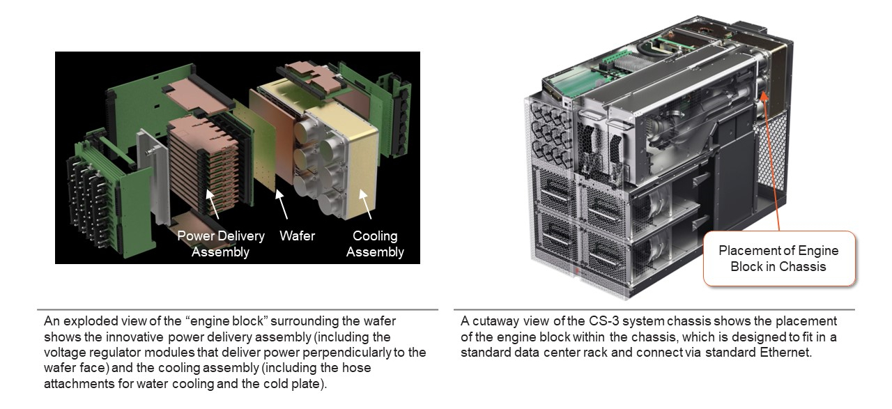
Cerebras develops wafer-scale AI processors. In its ITC complaint, Vicor states that Cerebras approached it in 2017 for a power system for WSE-1, and that Vicor has supplied vertical power delivery systems for WSE-1, WSE-2 and WSE-3.
According to the complaint, an array of 84 modules powers the WSE, with power flowing from a 54 V source above each module to the wafer reticle below. The complaint reports up to 30,000 A at 0.7 V and uses the patent’s Figure 11 to illustrate a 2 × 2 module array. It describes a multi-cell converter stacked with a Gearbox providing a capacitive layer, lateral connections and inter-digitation.
The patent itself describes a large semiconductor package carrying multiple converter assemblies. The Cerebras configuration and operating values are application details supplied by Vicor in the complaint, rather than measurements reported in the patent.
* This article explains how the technology is implemented. It does not interpret patent scope or assess infringement.